




















Cadence and Samsung Foundry are taking their long-running partnership into a more tightly integrated phase focused on second-generation 2nm manufacturing, and the framing is very clearly about one thing – making it easier to design extremely complex AI-era chips without getting slowed down by tooling and verification bottlenecks.
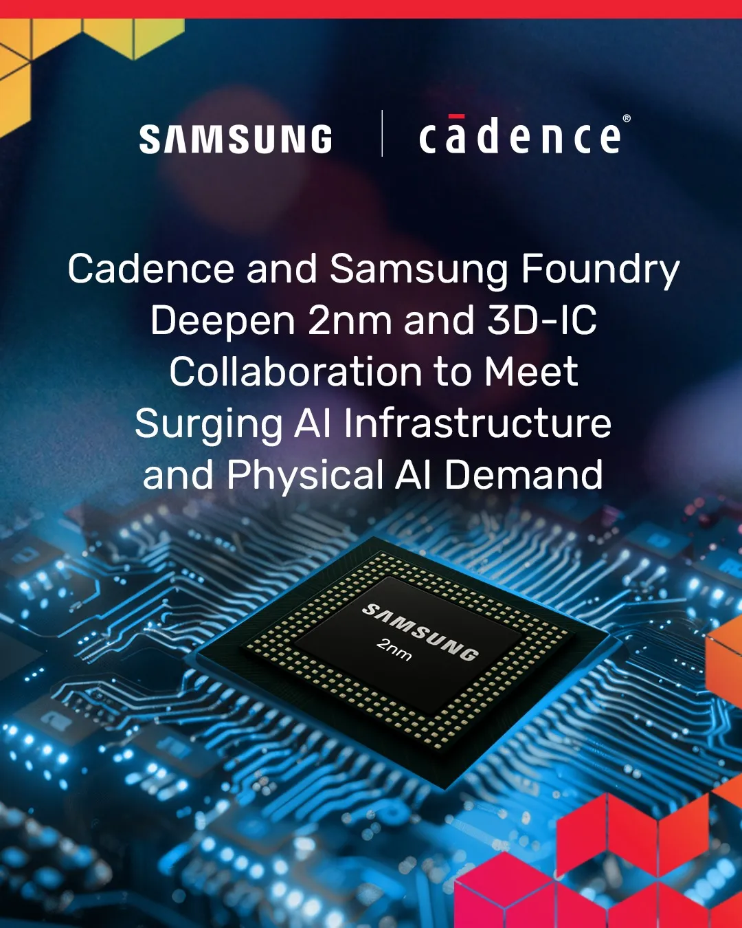
At the center of this expansion is a broader Memory and Interface IP portfolio from Cadence, now tuned for Samsung’s latest 2nm node. This includes high-speed connectivity standards like PCIe, UCIe, SerDes, and NVLink-C2C-enabled interconnect support, which is increasingly important as AI systems move toward chiplet-based and 3D-stacked architectures. Instead of single monolithic chips, modern AI hardware is becoming a network of tightly coupled dies, and the IP layer is what makes those connections physically and electrically viable.
Through agentic AI within design flows, EDA tools are no longer just passive simulation and layout systems – they are being positioned as semi-autonomous agents that can explore design spaces, optimize for performance, power, and area, and reduce the number of manual iterations required to reach tapeout. That shift matters because at 2nm, even small design inefficiencies can cascade into significant yield and performance impacts.
On the toolchain side, Cadence is pushing a fully certified stack for Samsung’s 2nm ecosystem, covering digital implementation, analog design, timing signoff, power integrity, extraction, and verification. The key industry implication here is tighter integration across these stages, reducing the traditional fragmentation that can lead to mismatches late in the design cycle when different tools and workflows are used.
For NVIDIA’s involvement in this partnership, they are providing GPU-accelerated EDA workflows and high-bandwidth interconnect technologies like NVLink-C2C; the ecosystem is effectively aligning chip design tools with the same compute paradigm that modern AI workloads already use. This creates a feedback loop where the tools used to design chips are themselves accelerated by the same class of hardware being designed.
At the edge, companies like Ambarella are applying this stack to next-generation low-power AI processors, where the constraint shifts from peak performance to efficiency per watt. Robotics, drones, and autonomous systems all depend on squeezing maximum inference capability out of minimal power envelopes, and advanced-node IP plus optimized design flows are what make that feasible.
Like our Facebook Page here at NasiLemakTech.com for more news and in-depth reviews! Also, join our Facebook Group for insightful information and memes!
Subscribe to our YouTube channel too!